


The Advantages of HDI PCBs and TEC’s Taxi film LED screen application
Click:
The Advantages of HDI PCBs and TEC’s Taxi film LED screen application
What is HDI PCB?
High-Density Interconnect (HDI) is simply a PCB with more number of interconnections, occupying minimal space. This results in the miniaturization of the circuit board. The components are placed closer and the board space is significantly reduced but the functionality isn’t compromised.
To be more precise, a PCB with an average of 120 to 160 pins per square inch is considered as an HDI PCB. The HDI design incorporates dense component placement and versatile routing. The HDI popularized the microvia technology. A denser circuitry is crafted with the implementation of microvias, buried vias, and blind vias. The drill to copper is reduced in an HDI design.
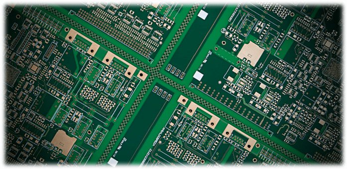
What Are the Advantages of HDI PCBs?
Phenomenal versatility: HDI boards are ideal where weight, space, reliability, and performance are primary concerns.
Compact design: The combination of blind vias, buried vias, and microvias brings down the board space requirement.
Better signal integrity: HDI incorporates via-in-pad and blind via technology. This helps in placing the components closer to each other which cuts down the signal path length. It therefore remarkably improves signal integrity due to shorter signal paths.
High reliability: The implementation of stacked vias make these boards a super shield against extreme environmental conditions.
Cost-effective: The functionality of a standard 8-layer through-hole board (standard PCB) can be reduced to a 4-layer HDI board without compromising the quality.
TEC's HDI PCBs in film LED screen?
Skyline-2.6, Pitch 2.6mm Taxi rear window film LED screen
Skyline-3.9, Pitch 3.9mm Taxi rear window film LED screen

点击右上角
分享给朋友吧


 Long by picture save/share
0
Add: Block 14, Tianliao No.5 Industrial Zone, Yutang Street, Guangming Dist, Shenzhen, Guangdong, China 518132
Follow TEC
Follow TEC